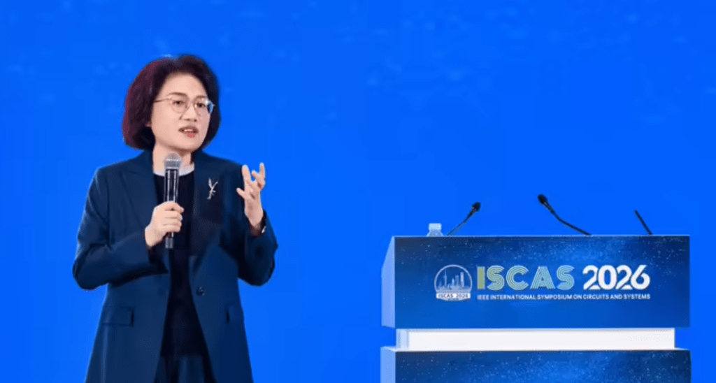

Huawei’s board member and head of its semiconductor business, He Tingbo, announced the company will launch a new Kirin smartphone chip using logic folding technology this autumn. The chip, expected to debut in the Mate 90 series in September, could give Huawei a competitive edge against Apple’s upcoming iPhone 18 lineup.
- What Happened at ISCAS 2026
- How Logic Folding Works
- The Tau Scaling Law and Future Roadmap
- Market Implications: Challenging Apple and the US Sanctions
- What This Means for the Industry
- Frequently Asked Questions
What Happened at ISCAS 2026
He Tingbo presented the new Kirin chip architecture at the International Symposium on Circuits and Systems (ISCAS) in Shanghai on Monday. The chip introduces logic folding — a technique that stacks logic structures into a dual-layer design rather than using a conventional single-layer layout. According to Huawei, this approach boosts transistor density and energy efficiency.
The chip will power Huawei’s Mate 90 series, which is slated for a September launch. He Tingbo explicitly positioned it against Apple’s iPhone 18 series, signaling that Huawei intends to compete head-on in the premium smartphone segment despite ongoing US export restrictions.
How Logic Folding Works
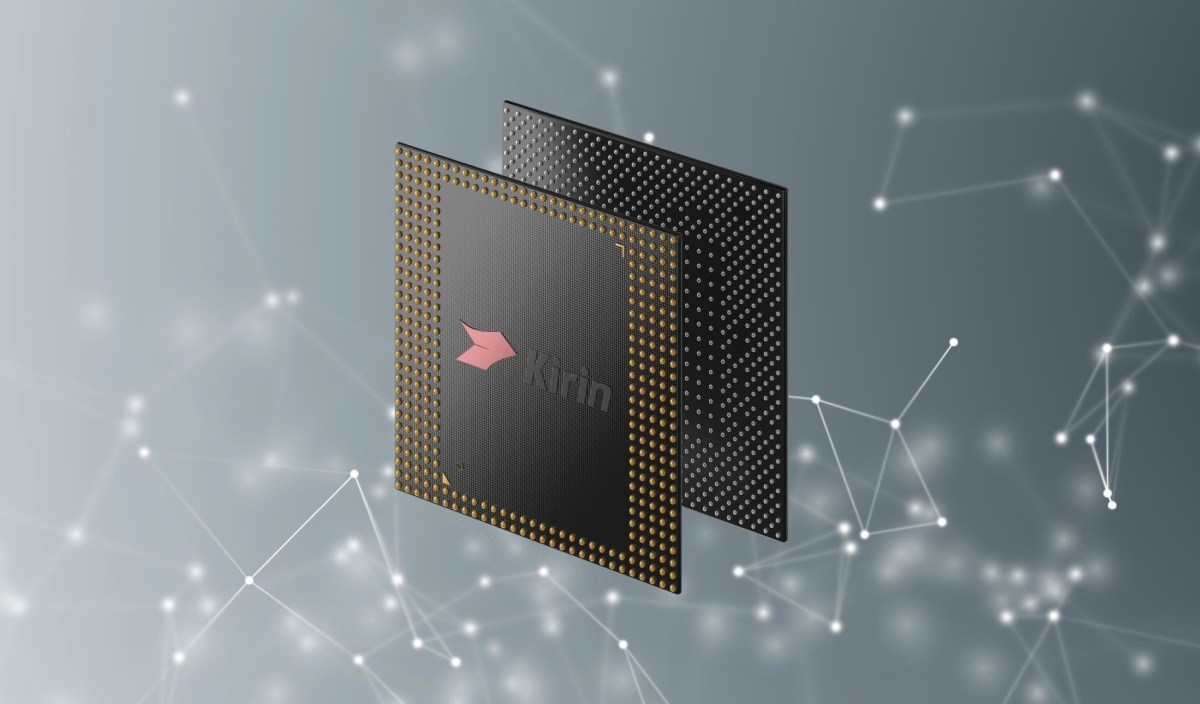
Traditional chip designs place all transistors on a single planar layer. As process nodes shrink, engineers run into physical limits — current leakage, heat density, and quantum tunneling. Logic folding breaks this by layering logic circuits vertically, effectively doubling the usable area without increasing the chip’s footprint.
Huawei claims the technique improves transistor density and energy efficiency simultaneously. While the company has not disclosed specific performance metrics for the new Kirin chip, early analyst estimates suggest it could rival the efficiency gains seen when the industry moved from 7nm to 5nm nodes.
The move is especially significant for Huawei because it cannot access advanced foundry nodes from TSMC due to US sanctions. The company has relied on its own HiSilicon design team and SMIC’s more limited process capabilities. Logic folding may help bridge the gap by extracting more performance from less advanced silicon.
The Tau Scaling Law and Future Roadmap
Alongside the chip announcement, He Tingbo introduced a new scaling framework called the Tau (τ) Scaling Law — also referred to as “Her’s Law” by colleagues. Huawei says the law defines how transistor density and energy efficiency evolve as logic folding matures.
Huawei projected that by 2031, high-end chips based on the τ Scaling Law will achieve a transistor density equivalent to 14 Å (1.4 nm) processes. That timeline puts it roughly a generation behind leading-edge foundries like TSMC and Intel, but it represents a concrete roadmap for a company that has been largely cut off from the global semiconductor supply chain.
The law is expected to apply beyond smartphones. Huawei indicated it will extend the design principles to AI computing, suggesting the company intends to build data center accelerators and edge AI chips using the same stacked-logic approach.
Market Implications: Challenging Apple and the US Sanctions
The Mate 90 series with the new Kirin chip will go head-to-head with Apple’s iPhone 18, likely launching within weeks of each other. For Huawei, this is a high-stakes return to the premium smartphone market it once dominated before US sanctions crippled its access to Google services and advanced chips.
If logic folding delivers the performance and efficiency Huawei claims, it could force Apple to accelerate its own chip innovation — or at least rethink its pricing strategy. It would also demonstrate that Huawei can continue producing competitive silicon without TSMC’s latest nodes, a proof point that other sanctioned or geopolitically constrained companies will watch closely.
However, the chip’s success depends on many unknowns: real-world power consumption, thermal management, and compatibility with Android app ecosystems (Huawei continues to use HarmonyOS, its own operating system, for the Chinese market). Global availability of the Mate 90 will also be limited by Google Mobile Services restrictions, meaning most sales will come from China.
What This Means for the Industry
For the broader semiconductor industry, logic folding is an important architectural shift. If Huawei proves it works at scale, other chip designers — particularly those facing foundry restrictions — may adopt similar techniques. The approach could also accelerate interest in 3D-IC (three-dimensional integrated circuits), a broader trend that includes stacking memory, logic, and sensors vertically.
For investors, the announcement reinforces that chip innovation is no longer solely tied to process node advances. Companies that can design clever architectures may compete with those who rely on the latest lithography. That dynamic favors design-heavy firms like Huawei’s HiSilicon, AMD, and Apple, while putting pressure on foundries to justify the rising cost of ever-smaller nodes.
Competitors like Qualcomm and Mediatek will need to monitor Huawei’s progress. If logic folding yields a 10-20% performance-per-watt advantage, it could shift the competitive landscape in Android chipsets. The iPhone 18, meanwhile, is expected to use an A19 chip built on TSMC’s 2nm process — setting up a direct comparison between different innovation strategies: advanced nodes vs. advanced architecture.
Conclusion
Huawei’s Kirin chip with logic folding represents a tactical response to a strategic problem: how to keep pace with Apple and other rivals when foundry access is restricted. The Mate 90 series will be the first real-world test of whether architectural cleverness can substitute for process leadership. If it works, it could reshape how the chip industry thinks about scaling — and whether the node race is the only path forward.